
|
 Home Home
 Projects Projects
 Experiments Experiments
 Circuits Circuits
 Theory Theory
 BLOG BLOG
 PIC Tutorials PIC Tutorials
 Time for Science Time for Science
|
| ||
|
24 February 2009 Author: Giorgos Lazaridis BJT Transistor theoryHow BJT transistors work Inside a transistor A BJT (Bipolar Junction Transistor) transistor has inside two similar semiconductive materials, and between them there is a third semiconductive material of different type. So, if the two similar materials are P and the middle one is N, then we have a P-N-P or PNP transistor. Similarly, if the two materials are N and the middle one is P, then we have a N-P-N material or NPN. Each transistor has 3 leads which we call base, collector and emitter, and we use the symbols b, c and e respectively. Each lead is connected to one of the 3 materials inside, with the base being connected to the middle one. The symbol of the transistor has an arrow on the emitter. If the transistor is a PNP, then the arrow points to the base of the transistor, otherwise it points to the output. You can always remember that the arrow points at the N material. These are the symbols: 
Transistor operation We will now explain the operation for the transistor, using an NPN type. The same operation applies for the PNP transistors as well, but with currents and voltage sources reversed. With no power applied to the transistor areas, there are two depletion zones between the two P-N contacts. Suppose now that we connect a power source between the base and the collector in reverse-bias, with the positive of the source connected to the collector and the negative to the base. The depletion zone of the P-N contact between the base and the collector will be widened. Moreover, a slight current will flow withing this contact (due to impurities). This current is the reverse contact current and we will use the symbol ICBO: 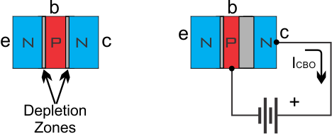
Now suppose that we connect another voltage supply between the emitter and the base in forward bias, with the positive of the source connected to the base and the negative connected to the emitter. The depletion zone between the emitter and the base will be shortened, and current (electrons) will flow when the voltage exceeds a specific level. This level depends on the material that the transistor is made of. Germanium (Ge) is the material that was originally used to make transistor, and later Silicon (Si) was used. For Germanium, the voltage is around 0.3 volts (0.27 @ 25oC), and for Silicon the voltage is around 0.7 volts (0.71 @ 25oC). Some of the electrons that go through the e-b depletion zone, will re-connect with holes in the base. This is the base current and we will use the IB symbol for reference. In real life, this current is at the scale of micro-amperes (üA or uA): 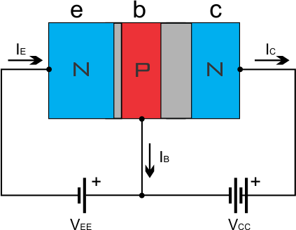
But most of the electrons will flow through the base (due to spilling) and will be directed to the collector. When these electrons reach the depletion area between the base and the collector, they will experience a force from the electric field which exists in this zone, and the electrons will pass through the depletion zone. The electrons will then re-connect with holes in the collector. The re-connected holes will be replaced with holes coming from the base-collector power supply (VCC). The movement of these holes equals to a movement of electrons in the opposite direction, from the collector to the supply. In other words, the current that flows to the emitter will be divided into the small base current and the larger collector current: IE = IB + IC Generally, the number of electrons that arrive at the collector is the 99% of the total electrons, and the rest 1% causes the base current. At the collector, except the electrons that come from the emitter, there is also the reverse current from the base-collector contact that we saw before. Both currents flow at the same direction, so they are added: IC' = IC + ICBO The following drawing shows how the electrons and holes flow within the transistor: 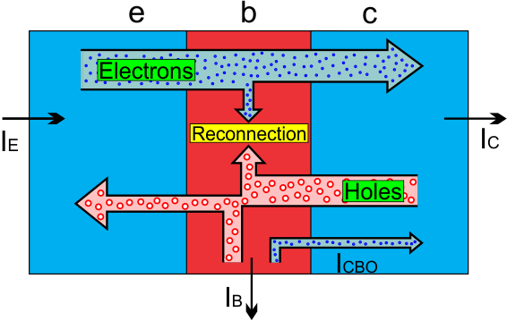
This is generally what happens inside a transistor when voltage is applied. The purpose of this theory is to explain how can someone use the transistor to design an amplifier or a switch, so we will not go into many details. It is enough to know this basic operation. The hybrid parameters [h] The hybrid parameters are values that characterize the operation of a transistor, such as the amplification factor, the resistance and others. They are used to calculate and properly use the transistor in a circuit. Most of the the hybrid parameter values are given in the datasheet by the manufacturer. You do not need to learn everything about hybrid parameters to design a transistor circuit, but it is good to know that they exist. Here is a quick reference: The hybrid parameters for Common Emitter (CE) connection Here is the first set of hybrid parameters for a transistor connected with Common Emitter. For now you do not have to worry about the type of connection. We will discuss them thoroughly in the next chapters. hie - input impedance The first hybrid parameter that we will see is the hie. This parameter is defined by the result of the division of the VBE by IB: hie = VBE / IB This parameters defines the input resistance of a transistor, when the output is short-circuited (VCE=0). hfe - Current Gain This is the most important parameter and is extensively used when calculating a transistor amplifier. This is actually the only parameter you need to know to begin designing amplifiers. The equation for this parameter is the following: hfe = IC / IB When we have the output of the transistor short-circuited (VCE=0), hfe defines the current gain of the transistor in common emitter (CE) connection. Using this parameter we can calculate the output current (IC) from the input current (IB): IC = IB x hfe This explains why this parameter is so useful. A BJT transistor has typical current amplification from 30 to 800, while a Darlington pair transistor can have an amplification factor of 10.000 or more. Another symbol for the hfe is the Greek letter ò (spelled "Beta"). hre - Dynamic transfer ratio reverse voltage This parameter is calculated with this equation: hre = VBE / VCE If the input of the transistor is open (IB=0) then this parameter gives the voltage gain when the transistor is connected with common emitter (CE). hoe - Output Conductivity This parameter is defined with the input open (IB=0) and the transistor connected in common emitter (CE) connection. The equation is: hoe = IC / VCE With the above conditions, this parameter defines the conductivity of the output. So, the impedance of the output can be defined as follows: ro = 1 / hoe = VCE / IC The hybrid parameters for Common Base(CB) connection hfb - Current Gain Like in Common Emitter connection, in Common Base connection there is a current gain ratio which is defined by the manufacturer with the hfb parameter. In this type of connection, the current amplification is almost 1 which means that no practical amplification occurs. hfb is also symbolized with the Greek letter ñ (Alpha). 0.9 < ñ < 1 The formula to calculate this parameter is the following: -hfb = IC / IE The hybrid parameters for Common Collector(CC) connection hfc - Current Gain As you understand, the current gain is the most important parameter in every type of connection. Same applies for the common collector connection. The equation is as follows: -hfc = IE / IB An alternative symbol for hfc is the Greek letter ó (Gama). Static and Dynamic operation As we saw above, the hybrid parameters begin with the letter h, and then a pointer follows to define which parameter we are talking about. If the pointer is written with lowercase letters, then this parameter refers to dynamic transistor operation. We call dynamic operation when the transistor operates with AC voltage, like for example in an audio amplifiers. If the pointer of the h parameter is written with capital letters, then the parameter refers to static transistor operation. The transistor operates statically if there is only DC voltage, like for example in a transistor relay driver. The current gain parameters have almost the same values in both static and dynamic operation. So, we can safely say that hFE is almost equal to hfe. Generally: hfe â hFE (hfe â hFE) hfb â hFB (hfb â hFB) hfc â hFC (hfc â hFC) For static operation, the alternative Greek letters can be used as well, with the pointer 0 or dc: hFE = ò0 = òdc hFB = ñ0 = ñdc hFC = ó0 = ódc Hybrid parameters are unstable One of the most common problems that a circuit designer faces when using transistors, is the fact that the h parameters are very sensitive to temperature changes. The most annoying thing about this is that the current gain changes dramatically. In common emitter connection for example, hfe can increase by 60% if the temperature climbs form 25 to 100 degrees. Take also into account that a transistor dissipates power in the form of heat, so temperature increment is something common that happens all the time. Another problem with hybrid parameters is that even between completely identical transistors, they may vary dramatically. You may have two transistors with the same code from the same manufacturer (completely identical) and yet one transistor may have hfe 150 and the other 300 (real measurement)! Within the next pages, we will see how can a designer work around with these problems. Transistor Circuit EssentialsBefore we start talking about the different types of transistor connections, we first need to declare some characteristic sizes and symbols that will be used from now on. IE is the Emitter current, IC is the Collector current and IB is the Base current. The direction of each current has to do with the type of the transistor (PNP or NPN). The voltage across two leads will be symbolizes by the letter V, with the two letters of the corresponding leads of the transistor as pointers. The second letter will always be the one that also characterizes the connection type of the transistor. So, for example, in Common Base connection, the voltage across the emitter and the base is VEB, and the voltage across the collector and the base is VCB. Similarly, in Common Emitter connection, VBE is the voltage across the base and the emitter and VCE is the voltage across the collector and the emitter. We will symbolize the power supplies of the leads with the letter V followed by the letter of the corresponding lead, twice. The symbol VEE is for the emitter supply, VCC for the collector supply and VBB for the base supply. Choosing the right connection There are 3 methods that a transistor can be connected, each one having advantages and disadvantages and specific application uses. So it is very important before you start designing your circuit, to be able to choose the proper connection according to your application requirements. First we will see these 3 connections in a glance, and then we will discuss each one thoroughly. The Common Base (CB) Connection in a glance 
A transistor is connected with Common Base, when the emitter-base diode is forward biased and the collector-base diode is reverse-biased, the input signal is applied in the emitter, and the output is taken from the collector. It is called "Common Base" because the input and output circuits share the base in common. The Common Base connection is probably the most rarely used type, due to the strange behavior that it has. As we saw in the operation of a transistor in the previous page, the emitter current is the strongest current of all within a transistor (IE=IB+IC). What this means is that the input of this circuit must be able to provide enough current to source the output. Moreover, the output current (IC) will be slightly less than the input current (IE). So this connection type is absolutely improper for a current amplifier, since the current gain is slightly less than unity (0.9 < hfb<1), in other words it acts as a current attenuator rather than a current amplifier. On the other hand, it does provide a small voltage amplification. The output signal is in phase with the input signal, so we can say that this is a non-inverting amplifier. But here comes another strange behavior: The voltage amplification ratio of this circuit is very difficult to be calculated, because it depends on some operational characteristics of the transistor that are difficult to be measured directly. The emitter-base internal resistance of the transistor for example and the amount of DC bias of the input signal play a major role in the final amplification ratio, but these are not the only ones. The current that flows within the emitter changes the internal emitter-base resistance which eventually changes the amplification ratio. This connection type has a unique advantage. Due to the fact that the base of the transistor is connected to the ground of the circuit, it performs a very effective grounded screen between the input and the output. Therefore, it is most unlikely that the output signal will be fed back into the input circuit, especially in high frequency applications. So, this circuit is widely used in VHF and UHF amplifiers. The Common Collector Connection (CC) in a glance (Emitter Follower) 
A transistor is connected with Common Collector, when the base-collector and emitter-collector diodes are forward biased, the input signal is applied in the base, and the output is taken from the emitter. It is called "Common Collector" because the input and output circuits share the collector in common. The common collector connection is used in applications where large current amplification is required, without voltage amplification. As a matter of fact, this circuit has the highest current gain factor. Remember that hfb=IC/IE (current gain in CB), hfe=IC/IB (current gain in CE) and hfc=IE/IB (current gain in CC). Taking into account that IE>IC (IE=IB+IC) and that IB is the smallest current, from the previous 3 formulas we can easily conclude that hfc>hfe>hfb. The current that this circuit can provide at its output is indeed the highest, and it it is the sum of the IC current plus the IB current from the input. The most distinctive characteristic though that this connection type has, is that the output voltage is almost equal to the input voltage. As a matter of fact, the output voltage will be equal to the input voltage, slightly shifted towards ground (VE=VB-VBE). This voltage drop depends on the material that the transistor is made of. A Germanium transistor has VBE=0.3V and a Silicon transistor has VBE=0.7 volts. So, the output signal on a silicon transistor will be exactly the same as the input signal, only that it will be shifted by 0.7 volts. This is why this connection is also called "Emitter Follower". The output signal is in phase with the input signal, thus we say that this is a non-inverting amplifier setup. This is a very efficient circuit to match impedance between two circuits, because this mode has high input impedance and low output impedance. It is widely used for example to drive the speakers in an audio amplifier, since the speakers have usually very low impedance. It is also used as a current amplifier in applications where the maximum current is required, such as driving solenoids, motors etc. This feature makes this type also perfect for designing Darlington pair transistors, since the maximum current amplification is the requirement. It is also a very effective circuit to make voltage regulators with high current supply. A Zener diode for example at the base of the transistor will provide a fixed voltage, and the output will be 0.7 (or 0.3) volts less than the Zener diode's regulation voltage, since it will follow the input, no matter how much current it provides. The Common Emitter (CE) Connection in a glance 
A transistor is connected with Common Emitter connection, when the base-emitter and emitter-collector diodes are forward biased, the input signal is applied in the base, and the output is taken from the collector. It is called "Common Emitter" because the input and output circuits share the emitter in common. This is the most common transistor connection used. The reason is because it can achieve high current amplification as well as voltage amplification. This results in very high power amplifications gain (P = V x I). Although -in maths- the current amplification of a Common Collector circuit is larger than a Common Emitter circuit, typically we can safely say that they both have almost the same gain: hfc = IE / IB hfe = IC / IB (1) IE = IB + IC (2) (1)(2)=> hfe = (IE - IB) / IB = IE / IB - IB / IB = hfc - 1 => hfe = hfc - 1 Suppose that a transistor has hfc=100 (in CC). From the above analysis we see that if we connect this transistor with common emitter, it will have hfe=99 (hfc-1), which is not a significant decrement. Additionally, the output voltage can also be predictably amplified. This is what makes this circuit so widely used. We will discuss this specific connection extensively with different biasing techniques. This mode is used in several applications, such as audio amplifiers, small signal amplification, load switching and more. A distinctive characteristic for this connection is that the output signal has 180 degrees phase difference from the input signal, thus we call it inverting amplifier. General Connection Characteristics Here is a table with the characteristic sizes of the 3 different transistor connections, so that you can directly compare them
Transistor Circuit Essentials Choosing the right bias After selecting the proper connection, the one that is most suitable for your application, you must select a biasing method. Biasing in general means to establish predetermined voltages and currents at specific points of a circuit, so that the circuit components will operate normally. For transistors, biasing means to set the proper voltage and current of the transistor base, thus setting the operating point, also known as quiescence point (Q). We will discuss in details the quiescence point within the next chapters. For now, you need to know that this point will determine how the transistor will operate (amplifier or switch). A correctly placed Q offers maximum amplification without signal distortion or clipping. The most efficient and commonly used biasing method for transistor amplifiers, it the voltage divider bias (VDB). We will analyze this method in detail, but first we need to discuss the other biasing methods. In this chapter, we will use a Common Emitter NPN transistor amplifier to analyze the various biasing methods, but each method can be used for other connections as well. Fixed bias 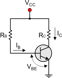 This is the most rarely used biasing method with transistor amplifiers, but it is widely used when the transistor operates as a switch. The base current IB is controlled by the base resistor RB. From the second law of Kirchhoff, we have: VCC = VB + VBE VB is calculated using the Ohm's law: VB = IB x RB So, by selecting the proper base resistor RB, we can define the required base voltage VB and base current IB. Now we can calculate the collector current using the appropriate hybrid parameter. Since this is a common emitter circuit, we use the hfe: IC = IB x hfe The problem with this method is that the collector current is very sensitive is slight current gain changes. Suppose for example that this is a silicon transistor and operates as a B-class amplifier with current gain 300, RB=80 Kohms, RC=200 Ohms and VCC = 10 volts: VCC = VB + VBE => VCC = IB x RB + VBE => IB = (VCC - VBE) / RB = (10-0.7) / 80000 = 112.25 uA IC = IB x 300 = 33.67mA The output of this circuit is taken from the collector resistor RC: VRC = IC x RC = 6.7 VoltsNow suppose that the temperature rises. As we've discussed in earlier pages, this will increase the current gain. An increment by 15% is a realistic and rather small value. From 300 it will climb up to 345. This means that the collector current will become 38.7mA, and the output voltage will also become 7.7 Volts! A whole volt higher than before. That is why this biasing method is not used for transistor amplifiers. On the other hand, due to the fact that this method is very simple and cost-effective, it is widely used when the transistor operates as a load switch, for example as a relay or LED driver. That is because the Q point operates from cut-off to hard saturation, and even large current gain changes have little or no effect at the output. Emitter feedback bias (Fixed bias with emitter resistor) 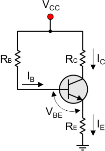 This is the first method that was historically used to fix the problem of the unstable current gain discussed previously. In a transistor circuit with fixed bias, a resistor was added at the emitter. This method never worked as it should, so it is not used anymore. This is how it was supposed to work. If the collector current is increased due to a temperature increment, the emitter current is also increased, thus the current through RE is also increased. The voltage drop across RE is increased (emitter voltage) which eventually increases the base voltage. Finally, this base voltage increment has as a result the decrement of the voltage across the base resistor RB, which eventually decreases the current of the base IB. The idea is that this base current decrement decreases also the collector current! This sounds amazing since a change of the output of the circuit has an effect on the input. This effect is called "feedback" and more specifically it is a "negative feedback", since an output increment causes an input decrement. Here is how the new collector current is calculated: IC = (VCC - VBE) / (RE + (RB / hfe)) Let's see how the previous circuit (Fixed bias) would react if we add a 100 Ohms RE feedback resistor. IC = (10-0.7) / (100 + (80000 / 300)) = 9.3 / 366.6 = 25.3 mA We assume again that the current gain is increased by 15%: IC = (10 - 0.7) / (100 + (80000 / 345)) = 9,3 / 331,88 = 28mA So, a 15% current gain increment caused a 15.1% output current increment. By adding a 100 Ohms feedback resistor at the emitter, a 15% current gain increment caused a 10.6% output current increment. The increment is 4.5% less which means that this method works somehow, but still the shifting of the Q-point is too large to be acceptable. Collector feedback bias (Collector to base bias) 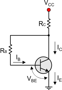 The next method that the researchers used to stabilize the Q point is the collector feedback bias. According to this method, the base resistor is not connected at the power supply, instead it is connected at the collector of the transistor. If the current gain is increased due to temperature increment, the current through the collector is increased as well, and this decreases the voltage on the collector VC. But the base resistor is connected at this point, so less current will go through the resistor in the base. Less current through the base means less current through the collector. Again, there is a negative feedback in this circuit. But how much is it? Lets do some math. The collector current is now calculated by the following formula: IC = (VCC - VBE) / (RC + (RB / hfe)) To see the change, we will apply this formula in our first example (fixed bias): IC = (10 - 0.7) / (100 + (80000 / 300)) = 9.3 / 366.6 = 25.3 mA When the current gain is increased by 15%: IC = (10 - 0.7) / (100 + (80000 / 345)) = 9.3 / 331.8 = 28 mA The effectiveness of this method compared to the emitter resistor feedback bias shown before is exactly the same. The difference is that, RC is usually much larger than RE, which results in higher stability. Nevertheless, quiescence point Q cannot be considered stable. Collector feedback bias (Collector to base bias) 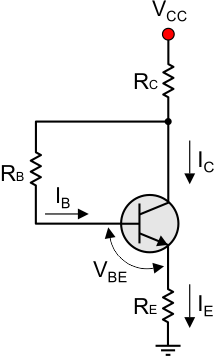 It did not take long before someone tried to utilize both the previous methods to work together to achieve better results. And indeed, the stabilization is much better than each one separately. The formula to calculate the collector current is the following: IC = (VCC - VBE) / (RC + RE + (RB / hfe)) Let's apply this formula to our previous examples IC = 9.3 / (100 + 100 + (80000 / 300)) => IC = 9.3 / 466.6 = 19.9 mA With a 15% current gain increment: IC = (VCC - VBE) / (RC + RE + (RB / hfe)) = 9.3 / (100 + 100 + (80000 / 345)) = 21.3 mA So, a 15% current gain increment causes a 7% output current increment. Although it is better than the previous circuits, still the Q point is not stable enough. Add to this that hfe is extremely sensitive to temperature changes and the transistor generates a lot of heat when it operates as a power amplifier. So we need a much better stabilization technique. Transistor Circuit Essentials Voltage Divider Biasing 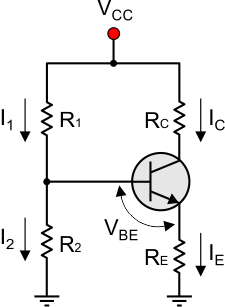 The most effective method to bias the base of a transistor amplifier is using a voltage divider. In the next chapter, we will analyze each transistor connection in detail and we will be using always this biasing method. Therefore, let's take some time to explain this method thoroughly. The idea is that the voltage divider maintains a very stable voltage at the base of the transistor, and since the base current is many times smaller than the current through the divider, the base voltage remains practically unchanged. The resistor Re provides the negative feedback as explained before (Emitter Feedback Bias). Due to the fact that the base voltage remains unchanged, the negative feedback works very effectively and any unwanted increment of the current gain produces an -almost- equal negative feedback. The collector and emitter currents change just a few, and the Q point remains practically stable. Now, let's see in detail how this works... Voltage Divider Bias Equations We start with the assumption that the base current (IB) is many times smaller than the current through the voltage divider (IVD). A ratio of 20 is a good approach. This means that the base current must be at least 20 times smaller than the voltage divider current. This condition allows us to exclude IB from our calculations, with an error less than 5%. Now we can safely calculate the base voltage as follows: VB = IVD x R2 Or using the classic voltage divider equation: VB = (VCC x R2) / (R1 + R2) The current that flows through the voltage divider is: IVD = VCC / (R1 + R2) From the base voltage we can calculate the emitter voltage and the collector-emitter voltage drop as follows: VE = VB - VBE VCE = VC - VE The emitter current is calculated using the Ohm's law: IE = VE / RE And since the collector current is practically equal to the emitter current, we can calculate all the transistor currents and voltages: VRC = IC x RC VC = VCC - VRC = VCC - IC x RC VCE = VCC - IC x RC - IE x RE = VCC - IC (RC + RE) As you see, we can calculate everything we need without using any hybrid parameter. This is an amazing and unexpected result. Two transistors with different current gains can operate as amplifiers with exactly the same amplification, only because they are biased with a voltage divider. Moreover, since VBE is many times smaller than VB and VB remains unchanged all the time, the emitter voltage VE remains also unchanged, hence maintaining a stable emitter current. Firm and Stiff Voltage Divider Previously, we made the assumption that the voltage divider current IVD is many times bigger than the base current IB, about 20 times as big. This is a good approach for an error less than 5%. This is not always possible thought. If the base current is high, the resistor values for the voltage divider must become very small, and this leads to numerous problems. In such cases, we design the voltage divider with a ratio of 10 instead of 20. This approach has an error less than 10% when the IB is excluded from the calculations, which is still acceptable. The voltage divider that satisfies this condition is named Firm Voltage divider: IVD > 10 x IB => RVD < 0.1 x òdc x RE (do not forget that ò = hfe) On the other hand, the application may require a very good Q stability with an error less than 1%. A ratio of 100 can be used to calculate the resistors, if this is possible: IVD > 100 x IB => RVD < 0.01 x òdc x RE The voltage divider that satisfies this condition is named Stiff Voltage divider, and has an error of less than 1%. Condition Confirmation Suppose that the designer wants to design a transistor amplifier with stiff voltage divider bias. He designed a circuit that has (along others) emitter current IE=1mA. The voltage divider he designed is calculated according to the stiff VDB condition, which means that the base current must be 100 times smaller than the voltage divider current. According to this calculation, the maximum base current cannot be greater than 40uA. The question now is: Does this circuit works efficiently for the whole hfe range? The fact that IB and hfe are excluded from the calculations, does not mean that these values do not affect the operation. They still have a small affect, but this is very small (1 to 10%). What we have to confirm now is that this affect will always remain small, even at the worst case scenario. But which is the "worst case scenario"? Well, simply: The worst case scenario is when the transistor operates with minimum current amplification. When this happens, the base current becomes maximum to supply the required emitter current. Suppose that the transistor that our designer used, has an hfe with range from 30 to 300. We have to confirm that the base current will remain under the calculated value (40uA) and still it will be able to provide full emitter current (1mA), even at the lowest hfe (30): IE = ò x IB => IB = IE / ò = 1mA / 30 => IB = 33uA So, the base current for the worst case scenario (33uA) is still less than the calculated base current (40uA), therefore we can say that this voltage divider remains stiff. What each part does Designing a transistor amplifier with VDB (Voltage Divider Bias) is not that hard, but sometimes it takes time to select the proper part values to begin with. And many times the designer has to change some parts to change the amplifier parameters. Here is a quick reference for the designer to know what each part controls: Output characteristic, Load Lines and Quiescence point There is a very interesting methodology to graphically analyze the operation of a transistor amplifier using the output characteristics and the load lines. By properly setting the quiescence point along the load line, one can select how the transistor amplifier will operate. For example, the same transistor can implement a Hi-Fi audio amplifier, B-class amplifier or a load switch, simply by setting the quiescence point onto different positions. The DC Load Line If you open a transistor datasheet, you will probably find a set of diagrams and characteristics. One of these is the Common Emitter output characteristic or IC to VCE characteristic and looks like this: 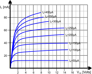
This is the IC to VCE characteristic of a BC547 transistor. The horizontal axis (x) has the VCE voltage in volts, and the vertical axis has the IC current, usually in milliamperes. Between them, there are several different curves. Each one of these lines corresponds to a different base current, usually measured in microamperes. From now on, we will work extensively with these characteristics, so it is important for you to understand how to read them and how to use them to determine the operation of the amplifier. The DC Load Line is a line that we draw on these characteristics, which eventually determines all the points that the transistor will operate at. In other words, the operation point (usually called Q from the word "Quiescence") will be somewhere on the DC load line. We use the term "DC" because -as we will see later on- there is also an AC load line. Many times, when we talk about the DC load line, we omit the term "DC" and we write only "Load Line" meaning the "DC Load Line". To draw this load line, we need to know the collector current and the collector-emitter voltage. Suppose for example that IC=40mA and VCE=12V. The load line is drawn with red color: 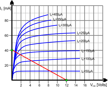
We will explain how to draw the load line, but before we do, we must first discuss about the 4 basic regions of this characteristic, the saturation area, the cut-off area, the linear area and the breakdown point. Region 1: The Saturation Area The saturation area is the area where the load line intersects with the saturation point of the characteristics. In the following drawing, we've marked the saturation area with a red transparent filter: 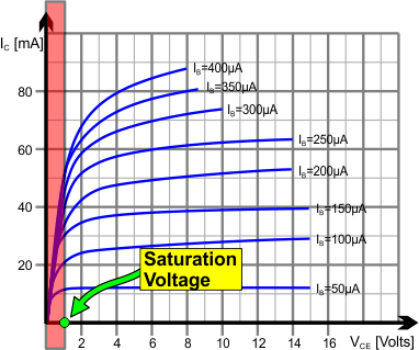
Due to the fact that the VCE potential is low at the saturation area, sometimes we consider that the saturation point is at the top of the load line (VCE=0) with a small error. Normally, the VCE voltage required to achieve saturation current is a few tens of a volt. This voltage is called "Saturation Voltage" and we use the symbol VCES. If the collector current is very high, the collector contact of the transistor is overheated and eventually the transistor is destroyed. Therefore, if the transistor is planned to operate at the saturation area -usually for switching applications-, caution must be taken to maintain the collector current bellow harmful levels. If the transistor operates as an amplifier and it is driven in the saturation area, then the output signal is distorted. That is because the transistor does not operate in it's linear areas. To avoid this, the transistor amplifier must be calculated in a way that the collector-emitter voltage will not fall bellow the saturation voltage. Generally: VCE > 0.5V => IC < VCC / RC Region 2: The Cut-Off area The cut-off area is the area in which the collector current becomes zero. In the following drawing, the cut-off area is marked with yellow mask: 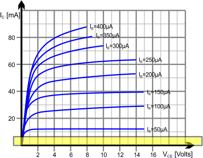
Generally, we can say that in order for a transistor to work in the cut-off area, the base current IB must become zero. This comes out of the IC to IB equation: IC = ò x IB The precise equation to calculate the cut-off point is this: IB = (ICO / (1-ñ)) + (ò x IB) ICO is the reverse saturation current. Since it is very small, usually around 10 to 50nA, we can safely remove it from the previous equation. When a transistor operates in the cut-off area, no current flows within the collector. Usually we drive the transistor in this area when we want it to operate as a switch. If the transistor operates as an amplifier, then the output signal will be clipped. Region 3: The Linear Area The linear area is the area between the cutoff and the saturation area of the transistor, as shown bellow with a green mask: 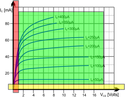
It is called "linear area" because in this area the transistor has the most linear operation. This area represents the normal transistor operation. To successfully design a transistor amplifier, the designer must be able to put the transistor to work within this area, otherwise the output signal will be either clipped or distorted. There are though special occasions where an amplifier operates beyond the linear area, such as a class-B or class-C amplifier. On the other hand, if the transistor operates as a switch, it must not operate within this area. A switch must be either ON or OFF, and this can only be achieved if the transistor operates in saturation of cutoff areas. Region 4: The Breakdown Point The breakdown point is the point on the VCE axis above which the collector current increases rapidly and the transistor is destroyed. This area is marked with a purple mask in the following drawing: 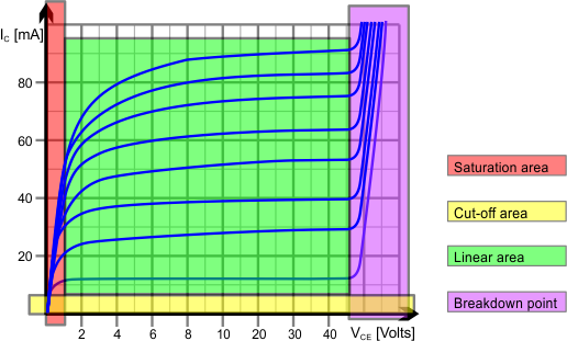
Output characteristic, Load Lines and Quiescence point How to draw the Load Line (DC Load line) To get a first clue about the Load Line, I will use an example with a Common Emitter amplifier with voltage divider biasing for the base. More details are yet to come for each connection type. Here is the circuit: 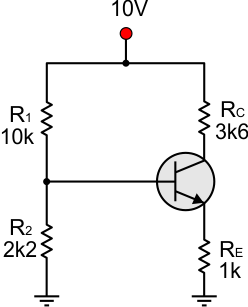
For an instance, let's forget about the input portion of the circuit (the voltage divider) and let's work only with the output portion. According to Kirchhoffs' law we have:  VCC = IC x RC + VCE + VE Let's now calculate the first point of the load line. This point (like any other point in a x-y Cartesian system) has 2 terms: an x and a y term. We need to find a VCE and a IC pair of values which corresponds to the x and y terms respectively. We can make this calculation much easier with a simple and common trick: We will calculate a VCE value for IC=0. This way, the first pair will be on the VCE axis. Let's solve the previous equation for VCE: VCE = VCC - IC x RC - VE First thing that we notice is that IC x RC is zero, since IC is zero. VE is zero as well, because IE is -almost- equal to IC, and VE is equal to IE x RE. The equation can be re-written as follows: VCE = VCC - 0 - 0 => VCE = VCC = 10V Now for the second pair. Similarly, we will calculate a IC value for VCE = 0. So, the second point will be on the IC axis. Let's solve for IC: VCC = IC x RC + VCE + VE = IC x RC + VCE + IC x RE = IC (RC + RE) + VCE => IC = (VCC - VCE) / (RC + RE) And since we defined that VCE = 0: IC = VCC / (RC + RE) = 10 / 4600 = 2.17 mA So, now we have the 2 points that we need to draw the load line. The points are: Point A (10, 0) Point B (0, 2.17) 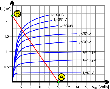
The green dots indicate the 2 points of the load line, and the red line is the DC load line itself. The Operation Point, AKA Quiescence point - Q We will continue the previous example and we will calculate the Q point. There is something that you need to make clear: The Q point is a point on the Load Line. The Load Line is calculated (as we saw before) by finding two points in the cut-off and saturation area. The Q point is usually placed within the linear area. The Q point is determined by the DC biasing of the transistor. The fact that the circuit uses VDB (Voltage divider Bias), allows us to neglect the base current in our calculations. So, the base voltage is: 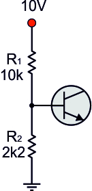 VB = VCC x R2 / (R1 + R2) = 10 x 2200 / 12200 = 1.8 V We can now calculate the emitter voltage as follows: VE = VB - VBE = 1.8 - 0.7 = 1.1 V And the emitter current is: IE = VE / RE = 1.1 / 1000 = 1.1 mA And since the collector current is almost equal to the emitter current, we can calculate the voltage drop across RC as follows: VRC = IC x RC = IE x RC = 1.1 x 3600 = 3.96 V Finally, the Collector-Emitter voltage is calculated as follows: VCE = VCC - VC - VE = 4.94 V Now we have everything we need to set the Q point: IC = 1.1 mA VCE = 4.94 V 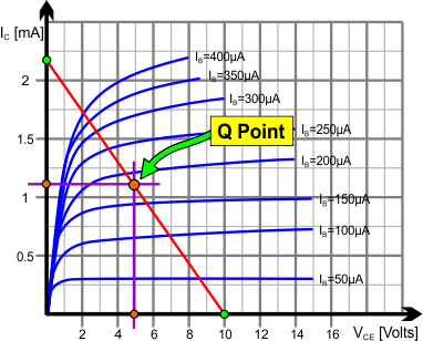
Let's analyze for one moment what we've done so far. First, we found two points to draw the load line. The first point was found on the VCE axis by zeroing the IC current, and the other point was found on the IC axis by zeroing the VCE voltage. Both points were calculated with the same equation: VCC = IC x RC + VCE + VE For the first point we solved this equation for VCE, and for the second we solved it for IC. Then, we calculated the Q point. For the Q point, we need another pair of IC-VCE values. These values are calculated from the DC transistor bias. If the DC bias is not in the cut-off or in the saturation area, then it must be somewhere on the DC load line that we draw before. That is true since both the load line points and the quiescence point are calculated with the exact same equation. The only difference is that for the load line, we choose (for our own ease and only) to find points on the two axis, whilst for the quiescence point we solve the equation for the DC values defined by the biasing resistors. Since the quiescence point is only one, and since the IC and VCE values of the quiescence point are critical, we usually use the pointer "q". So, for the quiescence VCE voltage we use the symbol VCEq, and for the quiescence IC current we use the symbol ICq. The Transistor operation in AC Until now, we've been talking only for transistors in DC operation. We've learned how to bias a transistor correctly, and we also saw a quick example on how to set the operation point. But many times, transistors are used to operate with AC signals. A transistor audio amplifier for example is an AC signal amplifier, since the microphone generally generates an AC output. And here is a point that many people confuse: Transistors are NOT AC components: Transistors can only operate with DC signals! That sounds kinda paradox, since we all know that transistors are also used to amplify AC signals. But think about this: Suppose that we have an NPN common emitter transistor amplifier, and we feed an AC signal at its base. As long as the input signal is higher than 0.7 Volts, it will be amplified normally and it will appear at the output of the amplifier. But what happens when the signal becomes less than 0.7 Volts? And worst, what happens when the signal becomes negative? As we know, an AC signal has a positive and a negative period. The answer is this: A negative signal at the base of an NPN transistor means that the base-emitter diode is reverse-biased. The diode acts like an open circuit (cut-off) and the amplifier does not work at all. There is also a tight limit: If the negative voltage become too high, the base-emitter diode will be destroyed. The maximum reverse voltage that this diode can handle is usually around 5 volts for small signal transistors. The exact value for each transistor can be found in the manufacturer's datasheet, usually with parameter name VEBO (Emitter-Base voltage). The same situation happens of course if we use a PNP transistor and we reverse-bias the base-emitter diode. So, how is it possible to amplify an AC signal? The answer is by biasing the transistor with DC voltage. Suppose for example that we want to amplify an 1 Vp-p AC signal. This means that the signal has +0.5 Volts positive period and 0.5 Volts negative period. If we bias the input with let's say 1.5 volts DC, then the input will vary from 2 Volts (1.5 + 0.5) to 1 Volt (1.5 - 0.5). This is considered as a DC signal and the transistor can amplify the complete period normally.
Coupling and Bypassing Capacitors As we said before, transistors are DC components. This means that the output will also be a DC voltage. But if we amplify an AC voltage, then we probably want to get an AC voltage at the output as well. How is this done? Simple, with a coupling capacitor. A capacitor operates as a resistor in AC and as an open circuit in DC. It is not the purpose of this theory to analyze in details the capacitor's behavior in AC and DC. Nevertheless, it is important to have some very basic knowledge about capacitors. The Coupling Capacitor A coupling capacitor is a capacitor connected in series with the circuit that we want to couple. The AC signal is free to go through the capacitor, while the same capacitor acts as an open circuit against any DC current. Let's see an example of a coupling capacitor: 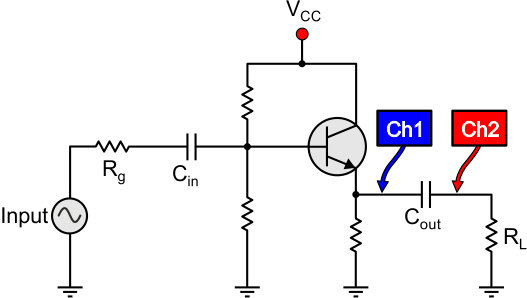
Both Cin and Cout are coupling capacitors. Their job is to block any unwanted DC voltage from between the stages that they couple. This is the what would appear in the oscilloscope's screen if two channels were connected, one before the Cout coupling capacitor (Channel 1-Blue line) and one after the same capacitor (Channel 2-Red line): 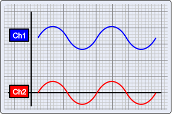
Looking at channel 1, it is obvious that the amplified AC voltage has been shifted above the zero line, and has become a DC voltage. That is because the DC voltage from the emitter of the transistor has been added to the amplified ÃC signal. Looking at channel 2, any DC voltage has been removed due to the coupling capacitor. It is possible only for the AC voltage to cross, and therefore it has become an AC voltage again. The Bypassing Capacitor A bypassing capacitor is a capacitor connected in parallel with a circuit that we want to bypass. Unlike the coupling capacitor, the bypassing capacitor removes any unwanted AC signal from this circuit, since any AC current goes through the bypassing capacitor, leaving only the DC current to go through the parallel circuit. Let's see an example: 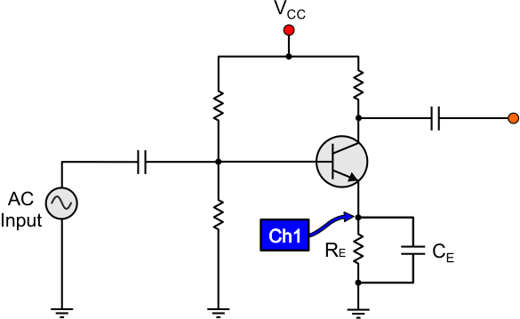
A bypass capacitor (Ce) is connected in parallel with a resistor (Re). What we want is to have only DC current flowing through the resistor, in order to maintain the current stable (Ie=Ve/Re). The actual problem is that when an AC signal is applied at the base of this circuit, this AC signal will also appear at the emitter of the transistor. This will change the emitter voltage which will eventually change the emitter current, and we do not want that. Therefore, we add the bypassing capacitor Ce. All the AC voltage will be grounded through this capacitor. Therefore, the voltage across the resistor Re will not change, and the current will remain stable. In the following graphs you can see what would appear in an oscilloscope's screen, if the probe was connected across Re. The left graph shows the output if Ce was NOT connected across Re, and the right graph shows the output with the bypassing capacitor Ce connected across Re: 
Choosing the right capacitor size In order for a coupling or bypassing capacitor to operate effectively, it must have the right size. As said before, the capacitor acts like a resistor in AC current. The resistance of a capacitor is called "impedance". Unlike resistors, capacitors do not have a fixed impedance. Instead, the impedance is determined by the frequency of the AC signal. The equation to calculate the impedance is the following: XC = 1 / (2*Ã*F*C) C is the capacitance in Farads, and F is the AC signal frequency in Hertz. So, a 10uF capacitor connected in series with a 1 KHz signal generator, will present an impedance of: XC = 1 / (2 x 3.14 x 1 x 103 x 10 x 10-6) = 15.9 Ohms So, what is the proper value for a coupling or a bypassing capacitor? There are two factors that must be taken into account: The frequency and the circuits total resistance. Let's talk about the frequency first. If the amplifier operates as a signal amplifier of a fixed circuit, then the answer is straight-forward: The frequency is the signal's frequency. But if the amplifier operates in a wide frequency range, then we must choose the worst case scenario. Let's see an example of an audio amplifier. Audio amplifiers typically operate from 20Hz up to 20Kz. To choose the right frequency for our calculation, we must first think what we want the bypassing or coupling capacitor to do: We want this capacitor to act as a short-circuit in AC currents. In other words, we want the capacitor to present the lowest impedance possible in AC current. Since the impedance XC is reverse-proportional to the frequency F, the lowest impedance is presented at the highest frequency. Thus, the worst case scenario (highest impedance) is presented at the lowest frequency. So, in our calculations we will use the lowest frequency that the capacitor will operate at. In an audio amplifier for example, the lowest frequency is 20Hz. The second factor is the total resistance of the circuit. Let's talk first for a coupling capacitor. In this case, we are talking about the total resistance of the circuit in series with the capacitor. Here is a simplified example of a circuit with a coupling capacitor: 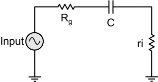
In this circuit, the total resistance is the sum of the internal resistance of the generator Rg, plus the internal resistance of the transistor ri. In a circuit with a bypassing capacitor, the total resistance is the total resistance of the circuit parallel to the bypassing capacitor. Here is a simplified example of a circuit with a bypassing capacitor. 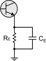
In this circuit, the total resistance is the RE. So, now we know how to choose the worst case scenario in terms of frequency, and how to calculate the total circuit resistance according to the capacitor type (coupling or bypassing). The optimum capacitor value that we choose must be 10 times smaller than the total circuit resistance, calculated for the worst case scenario. To calculate the capacitor, we solve the impedance equation for C: C = 1 / (2 * Ã * F * XC) Let's see an example. In the simplified example of a circuit with a coupling capacitor shown above, Rg is 50 Ohms. ri is 2.2 KOhms and the frequency is 20Hz to 20KHz. To calculate the optimum capacitor value, we must first calculate the total resistance of the circuit in series with the capacitor: Rtotal = 50 + 2200 = 2250 Ohms The worst case scenario is 20Hz (lowest frequency), so the capacitor must present a resistance of less than 225,0 Ohms (Rtotal/10) at 20Hz frequency: C = 1 / (2 * 3.14 * 20 * 225) = 35.3uF So, the capacitor must have at least 35uF capacitance. This makes sure that the capacitor will have less than 1% effect on the total resistance of the circuit. And since the calculated value does not exist as a standard capacitor value, we choose the next bigger value - in our case that is 47uF. DC and AC equivalents As we said previously, a transistor amplifier usually operates both with AC and DC voltages, the DC voltage is used to bias the transistor and the AC voltage is the signal that will be amplified. To analyze a transistor circuit, both voltages must be analyzed. But the transistor itself as well as the biasing components react differently in AC and DC signals. Obviously, there must be a method to analyze each signal separately. The simplest and most widely used method is using the DC and AC equivalents. According to this method, two equivalent circuits are extracted from the original circuit, the DC and the AC equivalent. The currents and voltages for each circuit are calculated separately, and then, using the superposition theorem we can calculate the final values. For your information, the superposition theorem states that: "The response -voltage or current- in any branch of a bilateral linear circuit having more than one independent source, equals the algebraic sum of the responses caused by each independent source acting alone, while all other independent sources are replaced by their internal impedances." Making the DC equivalent To make the DC equivalent circuit, the following steps must be taken: Suppose for example that we have the following circuit from which we want to make the DC equivalent: 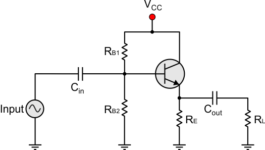
According to the first rule, all AC sources (if any) must become zero. This applies for the "Input" AC source that we have. When a power source becomes zero, it means that the output voltage will always have the same potential as the grounding signal - which is zero. Therefore we replace it with a grounding signal. According to the second rule, all capacitors must be replaced with an open circuit. CIN must be replaced with an open circuit, thus the Input AC supply can be omitted. COUT is also replaced with an open circuit, thus RL can be omitted. Here is the resulting DC equivalent circuit: 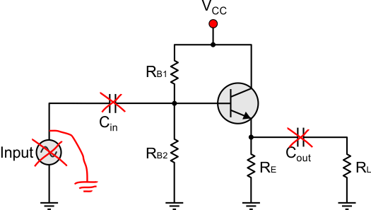
The above circuit can be simplified: 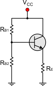
Having this circuit, it is very simple to make the DC analysis, since there is no AC source whatsoever. From this analysis, the designer is able to calculate all the DC biasing values, draw the DC load line and set the quiescence point. Making the AC equivalent To analyze the AC signals, we need to make the AC equivalent circuit. The following steps must be taken: When we designed the DC equivalent, we simple removed the AC sources. That is because the AC sources were coupled through decoupling capacitors, and due to the fact that all capacitors were replaced with open circuits, we simple removed the AC sources. But its not the same for the DC equivalent. The DC sources are directly coupled to the circuit so we cannot remove them. Therefore, according to the first step, all DC sources become zero. In other words, every component that is connected to the positive DC supply must be grounded. Then, we replace the capacitors with bridges: 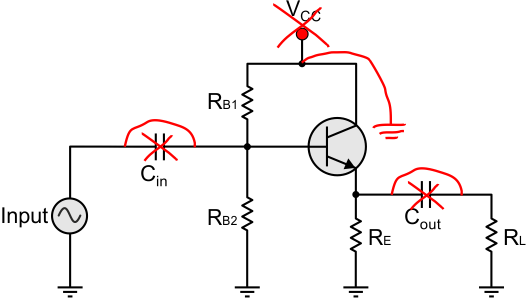
The above circuit can be simplified: 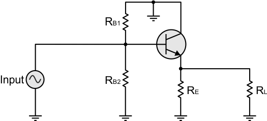
In many cases (like this one) the resulting circuit can be further simplified. The two resistors of the voltage divider are now connected in parallel, since the top side of RB1 is now grounded. Moreover, the emitter resistor and the load resistor (RE and RL) are also connected in parallel. We can calculate the equivalent resistors for RB1//RB1 and RE//RL and replace them in the circuit: 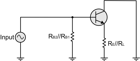
The above circuit is ready for the AC analysis since there is no more a DC source. The T and ÃÂ (II) models To analyze the AC transistor operation, we will use the T and ÃÂ models. These models are used to replace the transistor in the circuit. The transistor is replaced by the emitter resistor and a current source. The transistor T model Suppose that we have a Common Emitter transistor amplifier from which we've make the AC equivalent circuit as follows: 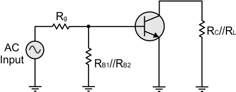
We can replace the transistor above with the T model. The circuit is then changed as follows: 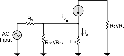
It is called "T model" because the transistor is replaced by a T-shaped circuitry. In our example you can locate this model if you search for this T-shaped circuitry rotated 90 degrees clockwise. The top side of the T has the collector current source, and the bottom side of the T has the internal AC emitter resistor. This resistor is marked with the symbol "r'e". The small "r" means that we are referring to an ac resistance, the "e" pointer means that we are referring to the emitter, and the prime symbol (') means that we are referring to an internal size of the transistor. As you see, the base AC voltage is directly applied across the internal base-emitter resistance. Therefore we can extract the following equation: ie = ub / r'e The input impedance of the base is this: Zin(base) = ub / ib Finally, from the collector's side, the ac collector voltage is calculated with the following formula: uc = ic x rc The symbol rc is the total AC collector resistance. The collector's resistance in DC operation is different than the AC resistance. That is because, in AC operation, the coupling capacitor adds the load resistance RL in parallel with the DC collector resistance RC. Therefore, we use the symbol rc in short for the total resistance RL//RC. The transistor ÃÂ (II) model Let's replace the transistor from the previous CE amplifier with the ÃÂ model: 
It is obvious why this is called àmodel. The letter àcomes from the Greek alphabet and is spelled like the letter "P". A double "I" letter can be used instead (II). From the T model, we know that: Zin(base) = ub / ib (1) And we also know that: ub = ie x r'e (2) (1)(2)=> Zin(base) = r'e x ie / ib But from the theory we know that ie / ib is the current gain ò. Therefore: Zin(base) = ò x r'e Both models can be used for the AC transistor analysis with the same results. If you happen to know the AC base voltage ub and the AC current ib, the T model can be then used to analyze the circuit, without needing to know the ò value. On the other hand, if the current gain ò is known, then you can use the àmodel for the analysis. The Base-Emitter AC internal resistance of the transistor (r'e) So far, we have seen how to do the DC analysis and the AC analysis separately, but we still do not know how the AC and the DC voltages are connected. The internal Base-Emitter AC resistance does exactly this: connects the emitter DC current with the base AC current. We use the symbol r'e which is different from the symbol re. The prime symbol shows that we refer to an internal size. The re is used for the AC external emitter resistance. The Base-Emitter internal AC resistance of the transistor depends on the DC current of the emitter. The equation which connects these two is this: r'e = 25mV / IE You may wonder what these 25mV are. The story goes back in 1947, when William Shockley invented the first transistor. Shockley used the diode current to determine the resistance: IE = IS (eVg/kT - 1) IS is the reverse saturation current and V is the voltage across the diode. At 25 oC, the above equation can be rewritten like this: IE = IS (e40V - 1) After some calculations, the equation becomes like this: r'e = 25mV / (IE + IS) And since IE is many times greater than IS: r'e = 25mV / IE The above equation is valid for operation at room temperature (25 oC). For an accurate calculation at different temperatures, the following equation can be used: r'e = (25mV x T+273) / (IE x 298) T is the contact temperature in degrees Celsius. Let's see now what this equation means. Suppose that we have a common emitter amplifier like the one we saw in previous pages, and we want to use the àmodel to calculate the transistor input impedance. Suppose also that we did the DC analysis with the help of the DC equivalent, and found that the emitter current is 1.1mA. From this DC current, we can calculate the AC base-emitter resistance: r'e = 25mV / 1.1mA = 22.7 Ohms Relative pages Comments
|
|
 Contact Contact
 Forum Forum
 Projects Projects
 Experiments Experiments
 Circuits Circuits
 Theory Theory
 BLOG BLOG
 PIC Tutorials PIC Tutorials
 Time for Science Time for Science
 RSS RSS
Site design: Giorgos Lazaridis © Copyright 2008 Please read the Terms of services and the Privacy policy |