|
 Home Home
 Projects Projects
 Experiments Experiments
 Circuits Circuits
 Theory Theory
 BLOG BLOG
 PIC Tutorials PIC Tutorials
 Time for Science Time for Science
|
| ||
|
The TRIS and PORT registers The PIC16f88 has 18 pins. Those are two sets of 8 I/O ports and the VDD / VSS pins for the power supply. Let's see how does Microchip draws the PIC pinout: 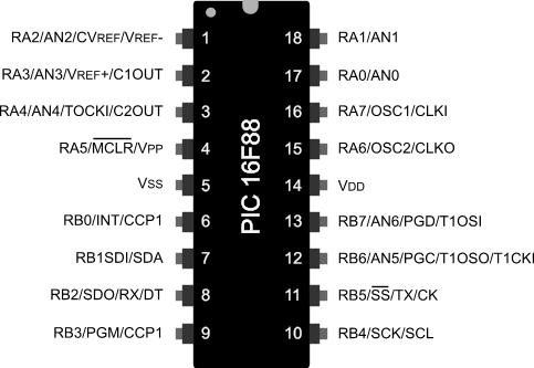
Except the power pins (#14 and #5), all others have more than one function. The first function that all pins have, is the RA or the RB function. This is the one that we will discuss at the moment. Taking a closer look to the above picture, you will notice that there are actually two sets of 8 ports, the RA0 through RA7 and the RB0 through RB7. These are our two main PORT registers. They are called PORTA and PORTB and you will deal with them all the time. So, what can you do with these ports? Suppose that you set the binary byte '11111111' to the PORTA register. If you have set the PORTA to be all outputs, then what will really happen is that all RA outputs of the PIC shall become '1'! Setting the type of the port pins (Input or Output) - The TRIS register Before you start playing with the port pins, you should declare their type. Each one can be Input or Output. There is also an analog state, but this will discussed on the advanced section. On power on of the PIC or after a reset, all ports become inputs. This is done to avoid driving an output pin directly to the VDD or VSS. To define the type of an I/O pin, you use the TRIS register. There are two TRIS registers, the TRISA and the TRISB that corresponds to the 8 pins of each port set, the A and the B. The TRIS registers are 8-bit registers. The LSB (Less significant byte) corresponds to pin #0 and the MSB (Most significant byte) to the pin #7. When one bit of this register is set to '1', the corresponding port pin shall become an input. When it is set to '0', then this port pin shall become an output. Let's see an example:
        bank1
        movlw b'00000001'
        movwf TRISA

        movlw b'11110000'
        movwf TRISB
        bank0
What someone would notice at the very first are the bank1 and bank0 macros. The TRIS registers are located in the bank 1. On the other hand, the PORT registers are located in the bank 0. I have experience many hours of hard mind-crashing debugging on my non-working programs, simply because i forgot to switch to bank 1 when setting the TRIS registers or because i forgot to switch back to bank 0. Once more, the bank 0 is the position with the most common registers. This is good because it saves you from switching between bank positions. But if you forger to check a register's bank position and fail to change bank, then funny results will happen The above code, will run as follows: The first line will switch to bank 1. The second line will load the binary number '00000001' into the W register. The third line will write the contents of the W register (00000001) into the TRISA register. This will set the type of port pins for the RA as follows:
The LSB bit of the number that was written into the TRISA register was '1', that is why the RA0 pin has become an INPUT. On the contrary, all other bits are '0', therefore, all other RA pins are outputs. Before you see the following table, try to imagine what will happen to the RB port pins. According to the program, the byte '11110000' was written in the TRISB register:
The first four bits are '0', therefore the pins RB0 through RB3 shall become OUTPUTS. The other four bits are '1' therefore the pins RB4 through RB7 are inputs. Controlling the ports - The PORT registers You have just learn how to set the type of the ports. Now you only need to learn how to control and use them. This is done by reading or writing bits to the PORT registers. The output state An output, is a port type where you can set HIGH or LOW ('1' or '0') it's state. If for example you wish to light an LED, you can connect it to one port and set it's state to '1' (HIGH). Suppose that we have the following code:
        bank1
        movlw b'00000001'
        movwf TRISA
        bank0

        movlw b'10000000'
        movwf PORTA
The first line will switch to bank1. The next two lines will set the type of the RA pins. Note the MSB bit. This is set to output, the RA7 is an output. Following we do not forget to switch back to bank 0. Then, we load the byte '10000000' to the PORTA register. If you notice the MSB bit, this is set to '1'. This means that the pin RA7, that is an output, will become HIGH. If an LED (and a resistor of course) was connected to this pin (pin #16), the LED would light. That is exactly the procedure how to set the port states. Alternatively, you can set or clear just one bit of a PORT register using the bsf and bcf instructions. The above program could have be written as follows:
        bank1
        movlw b'00000001'
        movwf TRISA
        bank0

        bsf PORTA,7
The fifth line is now changed. This line will set ('1') the seventh bit of the PORTA register. Two turn off this port, you need to set this bit to zero. You can do it either by writing with the movwf instruction a whole byte that has this bit 0 (for exmaple '00000000'), or by clearing this bit with the bcf instruction (bcf PORTA,7) The input state An input, is a port where you can read to your program the state of this pin. You can read this pin and find if it is conneted to HIGH or LOW state. Suppose that we have the following code:
        bank1
        movlw b'00000001'
        movwf TRISA
        bank0

        movf PORTA,W
The first line will switch to bank 1. The next two lines will set the RA pin types. The RA0 will become an input. We do not forget to switch back to bank 0. Then, at the fifth line, the PORTA register shall be read into the W register. Because the first (LSB) port was set to input, the LSB bit of the W register will become '1' IF the RA0 pin was connected to HIGH (VDD) or shall become '0' IF the RA0 was connected to LOW (VSS). If for example a push button was conencted to this pin, we could read the state of the pushbutton simply by reading the corresponding bit of the PORT register. Confirm your knowledge There is an online test to check your knowledge on this page. You may reveal the test with the following button: Comments
No part of this publication may be reproduced, stored in a retrieval system or transmitted in any form or by any means, electronic, mechanical, photocopying, recording, scanning or otherwise without the prior written permission of the author. Read the Disclaimer
All trademarks used are properties of their respective owners.
Copyright © 2007-2009 Lazaridis Giorgos. All rights reserved. |
  
|
 Contact Contact
 Forum
Projects
Experiments
Circuits
Theory
BLOG
PIC Tutorials
Time for Science Forum
Projects
Experiments
Circuits
Theory
BLOG
PIC Tutorials
Time for Science
 RSS RSS
Site design: Giorgos Lazaridis © Copyright 2008 Please read the Terms of services and the Privacy policy |